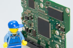
 The innovation of circuit boards have an entirely significant impact on how we approach technology design and manufacturing. They have supported majority of modern electronics. PCBs are inexpensive and are easier to produce in large quantities. They only need a little amount of work to bring pieces together upon receiving the components and boards.
Regardless if you just started to build your own design and create electronic devices, or just want to learn the basics of PCB layout, there are things you need first to consider. Understanding the appropriate steps in designing your PCB will leverage your work process and decrease any mistakes.
Here are the top 6 tips on how to optimize the layout of your printed circuit board.
1. Plan a PCB Layout as if You are Troubleshooting
No matter how keen you are when planning with your PCB layout, you will need to troubleshoot a circuit board at one point or another. If you plan your PCB layout as if you’re troubleshooting, it will be easier to solve any PCB issues that may arise in the future. This will make it easier for you to determine and solve any PCB issue if there are planning and troubleshooting aspects done.
You need to do a couple of things to make the procedure easier. First, ensure that all essential nodes are accessible easily. If there is some issue with your board, you will want to keep and isolate other board parts and work out for areas that are not working.
Adding a test point to your PCB layout is highly recommended by experts. Don’t worry, it’s not that complicated like how you’ve imagined. Test points only need to have a plated hole in your PCB. There are surely numerous complex ways of making a test point; however, for your layout, a simple one will work just fine.
2. There Must be Enough Spaces Between Segments
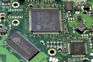
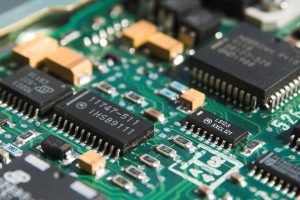
If your PCB is going to be mass-produced, it is important for it to be as efficient and inexpensive as possible, especially when it comes to designing it. it is also economical to pack as many components as you can into small spaces. However, this won’t be as smooth sailing as you think it is since there are quite a number of potential issues that may happen.
First things first, have sufficient space for you to add your wires. Each of the components must receive power from the main electricity cable. Generally, the majority of these components will be precipitated by every user action. This means you need to add more spaces for logic gates.
Make sure to leave some space for you to spread the wires in the event they become hot. Placing them together can end up messing with each other. Wires get hotter easily if they are not thick enough as well. Having extra spaces in between the wires will improve their auto-routing and soldering will be easier too.
PCBs that have a lot of pins will need more space than usual. You must take note of the amount of electromagnetic noise that PCB components will produce. Placing components right next to each other can make either component from working properly.
3. Select the Appropriate Software Design
There are a lot of choices available for your PCB design software. Some cost thousands and some are free. There are those that are downloadable via an installer, and there are those that are browser-based.
For browser-based software, it comes with multiple advantages. First, you can take advantage of saving your work automatically via cloud-based storage. With this, you don’t need to worry about your work getting lost or losing a huge amount of time because you forgot to save your design.
4. Make Use of Standard Orientation
Using standard orientation ensures that your components are properly oriented. For example, the first pin is located in the upper-right corner of the circuit board. Proper orientation guarantees that everything is arranged accordingly, the same way it will decrease any chance of improper soldering components.
Moreover, it will also help you with the troubleshooting in case you’re having problems with each component of the board.
5. Have a Blueprint of Your Components
Prior to starting to solder anything on your components, have a blueprint of your components and lay it down to ensure that everything will fit. Doing so will help you determine if some components you have are different from what you ordered. Or, if there were any mistakes on the datasheet you use as a reference.
Conclusion
PCBs are essential components of today’s technology. Regardless of the application, if you want your PCB to work properly, there are some things to consider. What we have here are just some of the basics that are essential to your PCB design process. Just like how meticulous we can get when it comes to choosing the best fiber optics cable manufacturer, this goes the same when selecting your PCB component supplier. High-quality components are a must. Not to mention that fiber optics and PCB are some of the important aspects in the world of network connection and modern technology.
References:
https://www.techmanik.com/7-tips-for-optimizing-your-pcb-designs/
https://www.tempoautomation.com/blog/5-tips-for-creating-the-best-multilayer-pcb-for-your-design/


Very come in handy. Cheers!
This is a very helpful info!
A lot thanks for sharing with us,
We are again come on your website,
Thanks and good day,
Please visit our site,