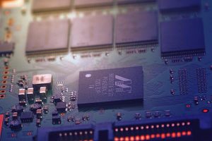
 Printed circuit boards underpin all our modern electronic devices. The evolution of the circuit board has had a profound effect on the way that we approach the design and manufacture of technology. PCBs are cheap and easy to mass-produce, and they require relatively little work to put together when you receive the boards and components.
Whether you are a hobbyist who is beginning to design and build their own electronic devices or want to learn about PCB design for the purposes of a future job, there are a few words of advice that you should keep in mind whenever you are designing a board. Approaching your designs the right way will optimize your workflow and reduce the rate of errors.
Choose the Right Design Software
The tools you use are sometimes just as important as the way that you use them. There are lots of options out there for PCB design software. Some are free while others are aimed at businesses and cost thousands of dollars. As well as downloadable software, there is also a growing number of browser-based options.
Using a browser-based tool comes with a number of advantages. First of all, by doing all of your work online, you can take advantage of automatic saving to the cloud. This ensures that you never have to worry about losing hours of work because you forget to save your project. One of the best options for PCB design is Gumstix and the Geppetto platform. With Gumstix, you can design your board quickly and easily and have it shipped to you in just 15 days.
Design with Troubleshooting in Mind
No matter how diligent you are or how much planning you do before you begin laying down your final schematic, you will inevitably need to troubleshoot a board at some point. When you do, you will find it much easier to diagnose and fix your issue if you have planned for it.
There are a couple of things you can do to make this process easier. First and foremost, make sure that all of your most important nodes are easily accessible. When you are having trouble with your board, you will want to be able to isolate the different parts of your board so you can work out which zones aren’t getting any power.
It is also a good idea to add a test point to your PCB designs. This isn’t as complicated as it sounds – a test point needs only to consist of a plated hole in your board. There are more complicated ways of creating a test point, but for your first designs, a simple one will suffice.
Ensure Sufficient Space Between Components
When you are designing a circuit board to be as cheap and efficient as possible, which is very important if they are going to be mass-produced, packing as many components as you can into a small amount of space might seem most efficient. However, this can also lead to a number of potential issues.
First of all, you need enough space to route all your wires. Every component needs to be able to receive power from the main power line. In most cases, these components will be triggered by user actions, which may mean you also need to add room for logic gates.
You also need to leave some room for the wires to spread when they get hot. If you place them too close together, they can end up interfering with one another. If you don’t set your wires to the appropriate thickness, they can end up getting far hotter than usual. Leaving some extra space will also improve auto-routing and make soldering much easier.
Components that have more pins will require more space. It’s also important to consider the amount of electromagnetic interference that components will generate. If you place certain components right next to each other, the interference can prevent either component from functioning properly.
Check Your Design with a Printout
Before you start soldering anything down, print out a blueprint of your components and lay your components down on it to ensure that everything is going to fit. This will also help you to identify if any of the components you have received are different from the ones you ordered or if there were any errors on the datasheet you were referring to.
Use a Standardized Orientation
The standard convention is to ensure that all your components are oriented so that the first pin, pin #1, is located in the upper-left corner. Ensuring that everything is oriented the same way will reduce the chances of you incorrectly soldering components down and will further help with your troubleshooting when you are having issues with individual components.
Reverse Wiring Direction Between Layers
You should have all the traces on one side of the board oriented horizontally while the other side is oriented vertically. This will help a great deal if you have any lines that need to cross one another at some point. If you are using multiple layers of traces within your board, alternate the orientation of the traces between layers.
Optimizing your design workflow will greatly improve your productivity and will also make it easier for you to approach new challenges. As you start to design increasingly complex boards, you will gain a greater appreciation for how much difference good design makes to the entire process. From laying down your initial idea to troubleshooting the finished board, following proper design practices makes everything faster and easier. Once you have the design of your boards down, you then need to find a reliable manufacturer to work with. All your design work is for nothing if you can’t trust the components you receive.
What do you think of these seven tips for optimizing your printed circuit boards designs? Think over your experience, and comment down below your best tip for those beginning in the field of PCB design.